FPGA Tutorial (Hello world UART monitoring & I/O control) (Part 1 Vivado)
In this tutorial, I will describe the step of creating a Hello world UART monitoring & I/O control application.
This article is a continuing tutorial from FPGA Tutorial (Hello world UART monitoring & I/O control) (Part 1 Vivado)
Step 9 Create a new Hello World Application Project
After set workspace directory from previous step Vitis program will launch new window as below.
The Zynq-7000 AP SoC Device Family
The Zynq-7000 AP SoC leverages the 28nm scalable optimized programmable logic used in Xilinx’s 7 series FPGAs.
The Z-7010, Z-7015, and Z-7020 leverage the Artix® -7 FPGA programmable logic and offer lower power and lower cost for high-volume applications.
The Z-7030, Z-7035, Z-7045, and Z-7100 are based on the Kintex® -7 FPGA programmable logic for higher-end applications that require higher performance and high I/O throughput.
Create an application for PS UART and UART Lite for communication testing on Xilinx Arty Z20
1. Open Vivado 2021.1 > Click File> Project >New
2. Create project name> PS UART and UART Lite
Create Pulse Width Modulation from VHDL
This topic is an example of how to create pulse width modulation work with the Zynq processing system.
Example PWM_VHDL.VHD VHDL code
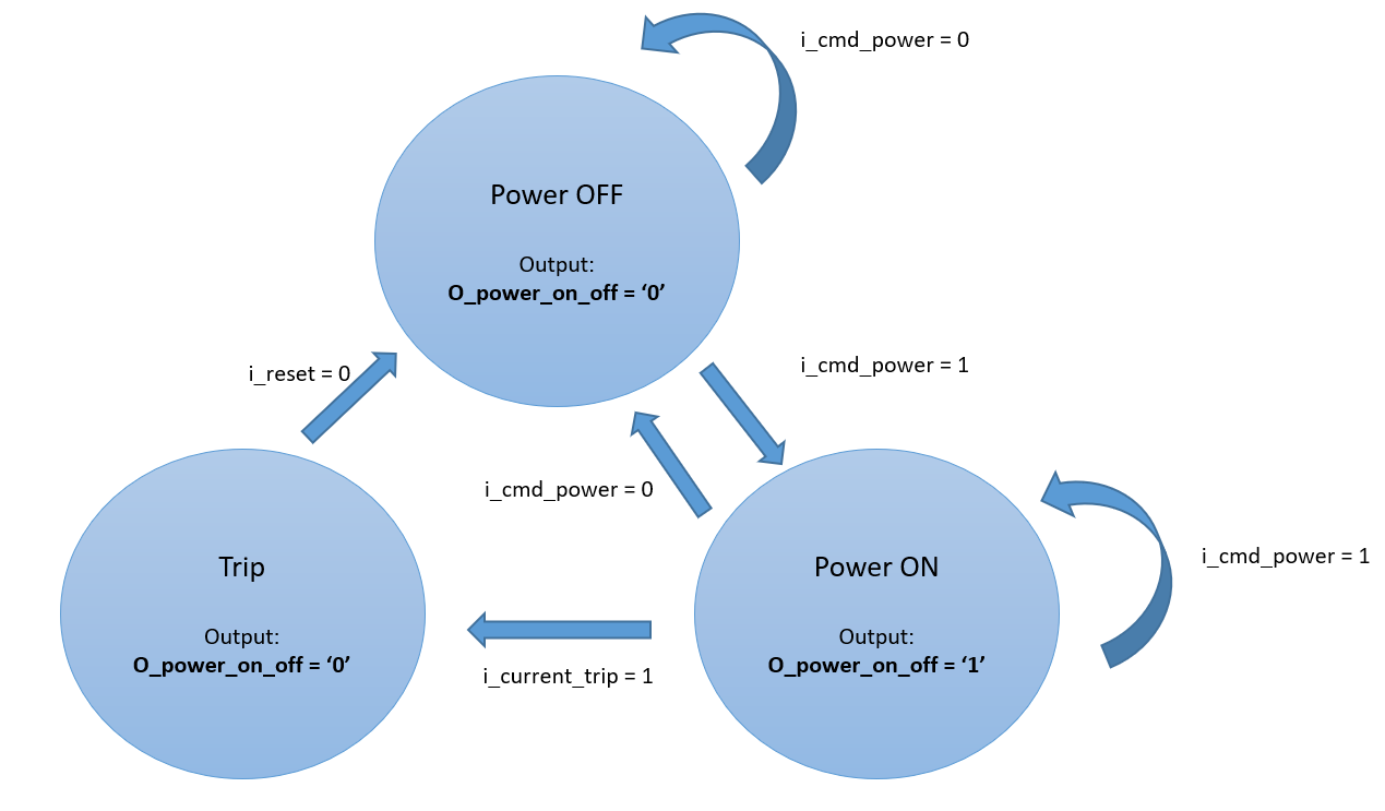
Finite State Machine(FSM) เป็นตัวช่วยในการออกแบบระบบวงจรดิจิตอล โดยใช้เทคนิคเขียนแผงผังการทำงานแบบ state ซึ่งทำให้เข้าใจขั้นตอนการทำงานของระบบวงจรดิจิตอลที่จะออกแบบได้ง่ายขึ้นและทำให้การเขียนโปรแกรมด้วยภาษา VHDL(Very High Speed Intregrated Circuit Hardware Description Language) ง่ายขึ้นด้วย
CAN is a communication protocol used in automotive and industrial control systems to allow devices to communicate with each other over a network. It is a robust protocol that is resistant to noise and interference, and it is widely used in a variety of applications.
Triple mode redundancy can be implemented in a Xilinx Zynq System on Chip by using the built-in redundancy features of Zynq's programmable logic (PL) and processing system (PS) components. This can be achieved by configuring the PL to implement triple modular redundancy (TMR) for critical logic and using the PS's built-in redundancy features to implement TMR for the processor and memory subsystems.
VHDL code for FPGA bitstream scrubbing for a Xilinx Zynq System on Chip would involve several steps, including:
Defining the VHDL architecture of the scrubbing module, which will include the logic for reading the bitstream, checking for errors, and correcting any errors that are found.
Writing the VHDL code for the scrubbing module, which will include the state machine and the error detection and correction logic.
Using MATLAB Simulink to generate HDL code for a Xilinx Zynq System on Chip would involve several steps, including:
Creating a Simulink model of the system, which would include the various blocks and subsystems that make up the design.
Configuring the Simulink model for code generation, which would include setting the target platform, specifying the clock, and other system-level parameters.
Verifying the Simulink model through simulation, to ensure that it is functioning correctly and meets the design requirements.