FPGA Tutorial (Hello world UART monitoring & I/O control) (Part 1 Vivado)
Overview
This guide will provide a step-by-step walk-through of creating a hardware design using the Vivado IP Integrator for the Arty Z7-20.
At the end of this tutorial you will have:
Created a simple hardware design incorporating the onboard LEDs and switches.
Created a .C project in SDK Xilinx Vitis 2020.1 testing the onboard LEDs and switches together using the hardware design shown in the previous step.
Created a .C project in SDK Xilinx Vitis 2020.1 print out UART message
General Design Flow
I. Vivado
1. Open Vivado 2020.1 and select ArtyZ7
2. Create a new Vivado Project
3. Create an empty block design workspace inside the new project
4. Add required IP blocks using the IP integrator tool and build Hardware Design
5. Validate and save block design
6. Create HDL system wrapper
7. Run design Synthesis and Implementation
8. Generate Bit File
9. Export Hardware Design including the generated bit stream file to SDK tool
10. Launch SDK Xilinx Vitis 2020.1
Now the Hardware design is exported to the SDK tool.
We will use SDK Xilinx Vitis 2020.1 to create a Software application that will use the customized board interface data and FPGA hardware
configuration by importing the hardware design information from Vivado.
II. SDK
Create a new application project and select the default Hello World template
Program FPGA and run application
Hello world UART monitoring & I/O control (PS)
* You have to install Vivado 2020.1, SDK Vitis 2020.1 and Digilent Board Files before following this guide.
You can refer installation guide here.
https://reference.digilentinc.com/vivado/installing-vivado/
1. Creating a New Project
When you first run Vivado this will be the main start window where you can create a new project or open a recent one.


2. Creating a New Block Design
2.1) Click to change Target language to VHDL.
2.2) Once the process has completed, click Create Block Design in the flow navigator.
2.3) Put the design name then click OK.
A blank Block Design will open up.

3. Add the Zynq IP & GPIO Blocks
3.1) Click the + Add IP button and search for ZYNQ. Double click on ZYNQ7 Processing System to place the bare Zynq block


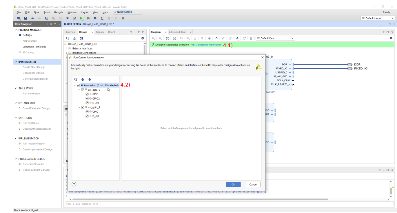
4. Run the Connection Automation Tool
4.1) Click Run Connection Automation
4.2) Click the All Automation then click Ok


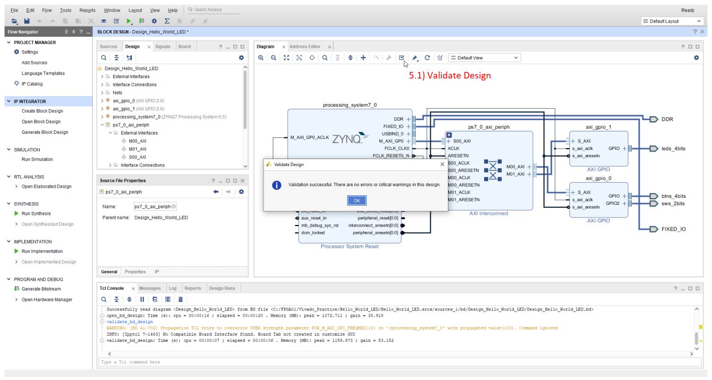
5. Generate HDL Wrapper and Validate Design
5.1) Select Validate Design. This will check for design and connection errors.

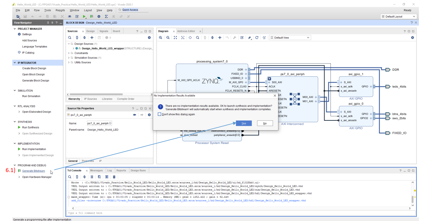
6. Generate the Bitstream
6.1) Click on Generate Bitstream at the bottom of the Flow Navigator. Wait for the process to complete and click OK.
If haven't done synthesis and implementation it will be asked to run within this process.
7. Export hardware files for SDK
7.1) Go to file→Export→Export Hardware
7.2) New window Export Hardware Platform show up, at Platform type select Fixed then click Next.
7.3) Next page check the box for Include bitstream then click Next
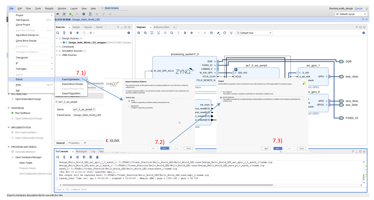

After click finish, Vivado will export hardware platform (C:/FPGA01/Vivado_Practice/Hello_World_LED/Design_Hello_World_LED_wrapper.xsa)

8. Launch SDK
8.1) Go to Tools→ Click Launch Vitis IDE

8.2) Vitis program will launch in a separate window and ask for a select workspace directory then click Launch